LEVVVEL
LEVVVEL
Loot
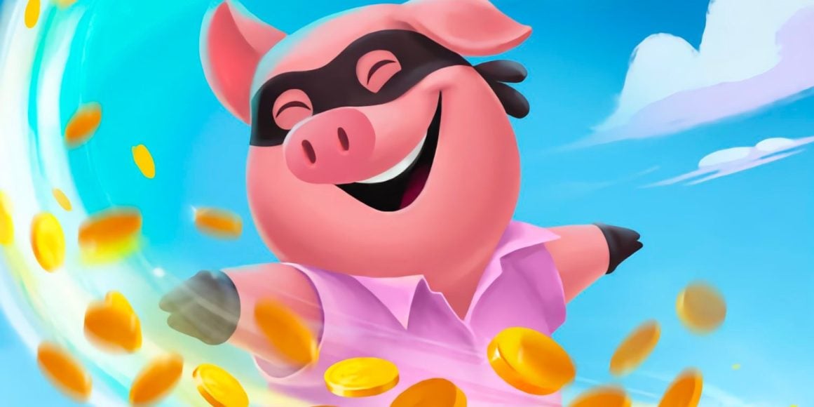
Coin Master free spins
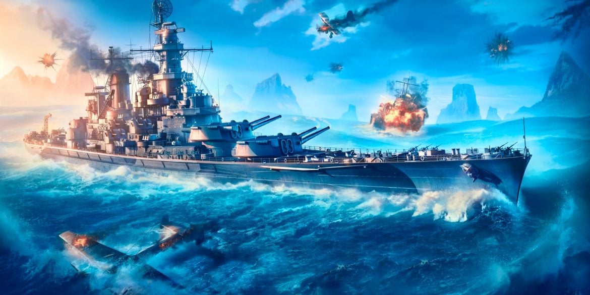
World of Warships codes
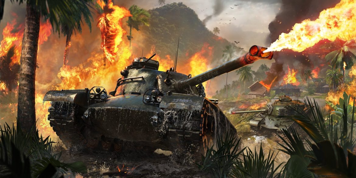
World of Tanks codes
Guides
Best free PC games
Best cross–platform games
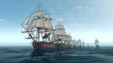
Best naval games
Best tank games
Best war games
Best WW2 games
Reviews
Statistics
Free Games
Today’s Coin Master free spins & coins links (April 2024)
World of Tanks codes April 2024
World of Warships codes April 2024
Best free PC games to play in 2024
Best cross–platform games to play in 2024
Best warship and naval warfare games to play in 2024
Best tank games to play in 2024
More games to play
Best games like Enlisted in 2024
Best games like Naval Action in 2024
Best games like Battlefield 1 in 2024
Best games like UBOAT in 2024
Latest figures
How many copies did Half-Life sell? — 2024 statistics
How many copies did Devil May Cry sell? — 2024 statistics
How many copies did Psychonauts sell? — 2024 statistics
How many copies did Thief sell? — 2024 statistics
How many copies did Quake II sell? — 2024 statistics
Load more
Loot
Coin Master free spins
World of Warships codes
World of Tanks codes
Guides
Best free PC games
Best cross–platform games
Best naval games
Best tank games
Best war games
Best WW2 games
Reviews
Statistics
Press ESC to close